Process FlowKorea Circuit is at the center of the smart world.
Pattern imaging(Outer layer)
It formulates a circuit by corroding copper foil: it formulates a circuit on a copper coated panel (exposure, development, corrison)
- Sub processes :
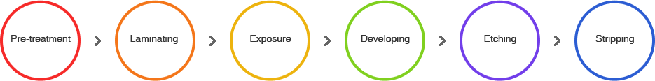
- Pre-treatment
- The oxidation layers or fingerprints are removed from the core(grinding, removal) and the copper layer surface is roughened to make sure that the dry film is well attached.
- Laminating
- This is a pre process to create a pattern on the PCB surface. Dry film is compressed by a heated roller.
- Exposure
- Work film is attached to the PCB where dry film is sprayed and a certain amount of light is used to make the monomer(single agent) turn into polymer, so that the pattern image can be created. UV is used to harden the necessary circuit area.
- Development
- The area not exposed to the UV during exposure has dry films; these can be removed chemically in this process.(Na2CO3)
- Etching
- After developing the core, the areas not covered by dry films (i.e. the copper layer) which does not correspond to the circuit is chemically removed.(FeCl3)
- Stripping
- After forming the circuit, dry film remaining on the PCB is chemically removed.(NaOH) (In the facility provided by our company, development, etching and stripping are connected in a line. The process is called D.E.S.)
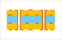
-
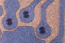
exposure
-
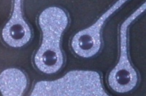
development
-
corrosion
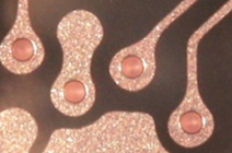
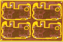
- Figure
- Product photos
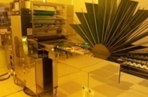
Process photos (main facility)
-
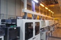
Pre-treatment
-
Laminating
-
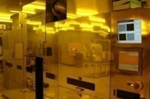
Exposure
-
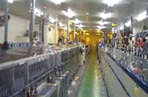
D.E.S