- Company Information
- Introduction to Products
- Introduction to Products
- HDI
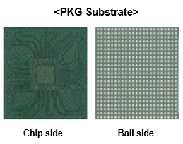
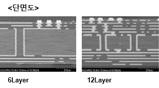
- Package Substrate
- Rigid-flex
- R&D
- ESG·Quality
- Ethical Management
- Ethical Management
- Code of Ethics
- Ethics pledge Guidelines
- human rights & labor policy
- IR

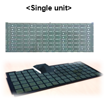
FCBGA connects the semiconductor chip and the package substrate with a flip chip bump. Fine align matching between layers is required due to miniaturization of substrate circuits and high multi-layers. In addition, large body size and multi-layer technology are required, especially for high performance computing. FCBGA is manufactured with a single unit flip chip substrate and is applied to servers and AI products.
Automotive, Server, AI, Switching, Micro-processor
| Dex-scription | Design | ||
|---|---|---|---|
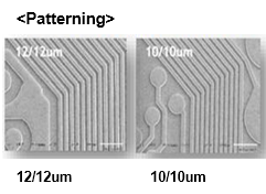
| Patterning | Line/Space | SAP | 9 / 12 |
| ISAP | 9 / 12 | ||
| Drilling | Via/Land | PTH | 100 / 200 |
| Laser | 60 / 85 | ||
| Bump | PAD | 95 | |
| SRO | 70 | ||
| Pitch | 130 | ||
| Die Bump Type | SAC 305, Sn0.7Cu | ||
| Surface Treatment | OSP+SOP, Immersion Tin | ||
