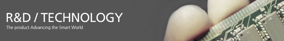
Status of Research CenterKorea Circuit is at the center of the smart world.

In addition, we have implemented the latest testing facilities to support technological development and improve our product technologies. Through academic/industrial collaboration and nationally funded projects, we are striving to develop the technologies that can lead the industry.

Research center status
- Date of establishment: Nov 03, 1990
- Korea Circuit research center
- Address: 133-9(Seonggok-dong) Gangchon-ro Danwon-gu, Ansan-si, Gyeonggi-do
- Research area: (electrical, electronics) PCB
- Approval no.: 19901113
- R&D head: Yang Deok Jin
- # of materials: 35
Main history
- 1990
- 1990.11Established the R&D center.
- 1991~1998
-
PCB Research Union
– Completed development of the five R&D projects for the industry.
- 1991.08 ~ 1992.07Developed the impedance board.
- 1991.08 ~ 1993.11Developed the multi-layered PCB.
- 1992.11 ~ 1995.10Developed the ultra precision thin layer PCB.
- 1995.12 ~ 1997.11Developed the MCM-L PCB.
- 1996.11 ~ 1998.10Developed the conductive PASTE PCB.
- 2005
- 2005.05Member of KPCA (Korea PCB Association)
- 2007~2024
-
Government funded projects (national projects)
- 2007.07 ~ 2011.06Developed the next-generation multi-functional embedded SoP_L technology.
- 2007.09 ~ 2008.08Developed the technology for semiconductor packages with the PCB having built
in chips.
- 2009.09 ~ 2011.08Improved mechanical/thermal reliability of the SiP Module.
- 2010.06 ~ 2013.05Developed the next-generation ultra thin layer MCP PCB module/SiP embedded
PCB module.
- 2010.07 ~ 2012.06Developed the Rigid-Flexible photoelectric PCB integration technology.
- 2011.11 ~ 2013.10Developed the highly integrated Hole Plugging Ink product.
- 2013.11 ~ 2014.11Developed the thin layer capacitors for highly dielectric compounds based
embedded PCB.
- 2020.04 ~ 2023.12Developed the technology for producing a titanium drum electrode with a thickness of
0.7 μm or more and a diameter of 3.5m for microcircuit
- 2020.08 ~ 2022.12Developed the 4N class palladium materialization and high reliability palladium plating
technologyfor semiconductor electronics industry from electronic scrap
R&D facility
15 cases other than the non destructive precision tester (X-Ray inspection equipment).