Process FlowKorea Circuit is at the center of the smart world.
PSR Photo Solder Resist
Using non changeable ink, the non usable areas are coated.
- Sub processes :
-
- Permanent Ink is coated on the plated PCB to protect the circuit. This prevents the occurrence of solder bridges between the circuits in the next process – surface processing and part mounting.
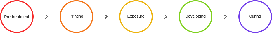
- Pre treatment
- In addition to the removal of oxidation layers and oils that can degrade the adhesion of ink to the PCB surface, by providing roughness to the copper surface of the PCB, we can improve the adhesion of ink to the copper in the printing process.
- Printing
- It sprays ink on the surface of a board built with circuits to protect PCB's surface mounted circuit from the outside materials. It includes two coating techniques: Screen Coating and Spray Coating Techniques
- PSR exposure
- There are areas that play the role of register for the printed ink and the area to be exposed (soldering/ gold plating). These areas are exposed to the UV light through exposure film, so that they can be selectively photo hardened.
- PSR developing
- If there is an area that has not been hardened as it was not exposed to UV light, developing liquid is used to remove the register and expose the copper.
- Curing
- After the PSR developing process, hot air is blown on the product to completely harden the PSR ink.
- Figure
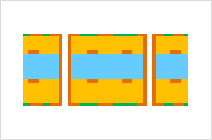
- Product photos
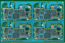
Process photos (main facility)
-
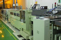
Pre-treatment
-
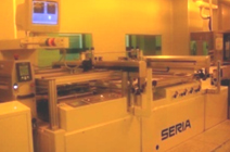
Printing
-
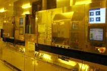
Exposure
-
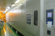
Developing
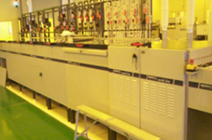
-
Curing