
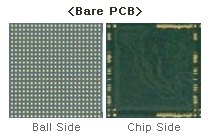
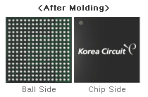
CSP(Chip Size Package)는 Package Substrate 중에서 Substrate 의 크기가 반도체 Chip 크기의 120%를 넘지 않는 제품을 칭하는 표현입니다. 면적 축소를 위해 CSP는 일반적인 BGA에 비해서 배선 밀도가 조밀하게 형성됩니다. CSP의 가장 큰 목적은 실장면적의 축소에 있습니다.
- Memory, analog, ASICs, Logic, RF devices
- Notebook, Subnotebook, Personal Computers
- GPS, PDA, wireless telecommunication system
| Item | Design | ||
|---|---|---|---|
| Patterning | Line/Space | MSAP | 16 / 16 |
| Subtractive | 25 / 25 | ||
| Drilling | Via/Land | PTH | 75 / 180 |
| Laser | 65 / 125 | ||
| Ball Pad Pitch | 0.4 mm | ||
| Solder Mask Tolerance | ± 7 | ||
| Strip Size | 240 X 95 mm | ||
