
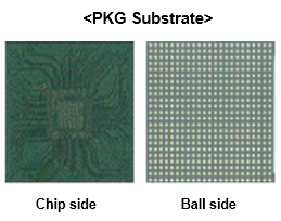
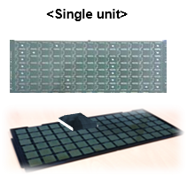
FCBGA는 반도체 칩과 패키지 기판을 Flip chip bump로 연결하며 기판 회로의 미세화 및 고 다층에 따른 층간 미세 정합이 요구 되고 특히 High Performance computing 대응을 위해 Large Body size, 고 다층 기술을 요구 합니다. 그리고 Single unit flip chip substrate로 제작 하고 Server, AI 제품에 적용 됩니다.
Automotive, Server, AI, Switching, Micro-processor
| Dex-scription | Design | ||
|---|---|---|---|
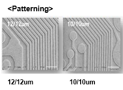
| Patterning | Line/Space | SAP | 9 / 12 |
| ISAP | 9 / 12 | ||
| Drilling | Via/Land | PTH | 100 / 200 |
| Laser | 60 / 85 | ||
| Bump | PAD | 95 | |
| SRO | 70 | ||
| Pitch | 130 | ||
| Die Bump Type | SAC 305, Sn0.7Cu | ||
| Surface Treatment | OSP+SOP, Immersion Tin | ||
