
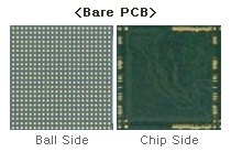
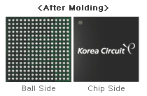
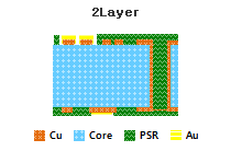
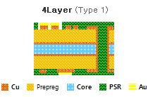
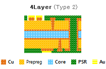
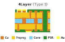
CSP(Chip Size Package) is a product whose package substrate size does not exceed 120% of the semiconductor chip size. To reduce the area size, the CSP with highly dense wiring compared to general BGA is formed. The most important goal of CSP is to reduce the mounting area size.
- Memory, analog, ASICs, Logic, RF devices
- Notebook, Subnotebook, Personal Computers
- GPS, PDA, wireless telecommunication system
| Item | Design | ||
|---|---|---|---|
| Patterning | Line/Space | MSAP | 16 / 16 |
| Subtractive | 25 / 25 | ||
| Drilling | Via/Land | PTH | 75 / 180 |
| Laser | 65 / 125 | ||
| Ball Pad Pitch | 0.4 mm | ||
| Solder Mask Tolerance | ± 7 | ||
| Strip Size | 240 X 95 mm | ||
