
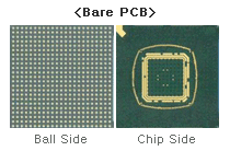
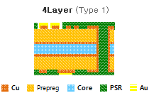
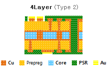
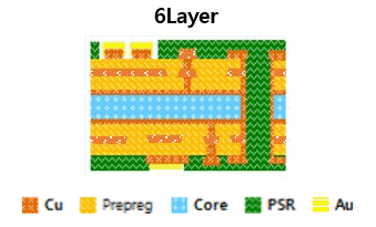
PBGA(Plastic Ball Grid Array) expresses the structural characteristics of the Package Substrate. In other words, on the back of the PCB, instead of leads, solder balls are lined up to connect the substrate to the main board. The term PBGA is used as generally as the Package Substrate.
-. ASIC, DSP and Memory, Gate Arrays
-. Microprocessors / Controllers / Graphics
-. PC Chipsets and Peripherals
-. Graphics Processors
-. Set-Top Boxes
-. Game Consoles
-. Gigabit Ethernet
| Item | Design | ||
|---|---|---|---|
| Patterning | Line/Space | Subtractive | 40 / 40 |
| Drilling | Via/Land | PTH | 150 / 300 |
| Thickness | 560 ± 40 | ||
